

Irina V Antonova
Institute of Semiconductor Physics, Russia
Title: Graphene/fluorinated graphene systems for a wide spectrum of applications
Biography
Biography: Irina V Antonova
Abstract
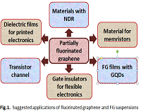
In the report we consider the properties of partially fluorinated graphene (FG) created with the use of a simple fluorination method based on the treatment in an aqueous solution of hydrofluoric acid. FG films can be formed from CVD grown graphene and a graphene suspension. A possibility to control a size of graphene flakes in a suspension in the course of their fluorination was also demonstrated. The possibility to create the FG films with arrays of graphene quantum dots (GQDs) is revealed. The spectrum of quantum confinement levels for GQDs in a fluorinated matrix and a charge relaxation time from GQDs are determined with the use of charge transient deep level spectroscopy. The time of GQD recharging can be controlled by means of GQD thickness variation or daylight assistance. This finding makes films with GQDs promising for flash memory applications. Fluorination of domain boundaries leads to a strong current modulation by gate voltage with an ON/OFF relation ~105 (the property important for field-effect transistors). The negative differential resistance (NDR) and a step-like increase in the current are found for films created from the fluorinated graphene suspension. The NDR resulting from the formation of a potential barrier system in the film is observed for a relatively low fluorination degree. The observation of NDR in FG films widens the range of possible applications. A stable resistive switching effect is detected in films created from the FG suspension. The origin of resistive switching was found to connect with the appearance of traps with energy 0.08 eV and the recharging time lower than 700 ns. The charges in metal–insulator–semiconductor structures with FG dielectric layer have been estimated as the ultra-low values of (0.5–2) x1010 cm-2. Suspensions of fluorinated graphene with nanometer size flakes are of interest for the development of 2D ink-jet printing technologies and the production of thermally and chemically stable dielectric films for nanoelectronics on rigid and flexible substrates.