

Adam Khan
AKHAN Semiconductor Inc., USA
Title: Thin film nanocrystalline diamond for optical and monolithically integrated display applications
Biography
Biography: Adam Khan
Abstract
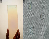
Diamond is well-known for its extreme hardness, high- optical transparency, high thermal conductivity, and great chemical stability. In spite of all these excellent properties, diamond has largely been absent in optical applications due to the difficulty in fabricating high quality diamond thin films at lower substrate temperatures cost efficiently. Pioneering work on low temperature, high quality diamond deposition methods by AKHAN Semiconductor Inc. has opened doors for the use of diamond in a wide variety of optical applications. Nanocrystalline Diamond (NCD) coatings with grain size of 10-100 nm can significantly enhance the breakage, scratch performance and hydrophobicity of glass displays and lenses. In this work, NCD thin films of 50-250 nm thickness were deposited on commercial BK7 glass and chemically hardened Aluminosilicate Glass (Gorilla Glass) substrates (Figure 1 (a & b)) using Hot Filament and Microwave Plasma Chemical Vapor Deposition (HFCVD and MWCVD) techniques under optimized substrate temperatures to avoid substrate deformation. Optical characterization work of the as deposited NCD films was preformed using ellipsometry, spectral reflectance and spectrophotometry over visible wavelengths. Mechanical characterization work was also performed to obtain hardness & Young’s Modulus data for the NCD films. Measured results demonstrate the viability of NCD as a protective coating for a broad range of optical applications. Additionally, low temperature, high quality diamond deposition allows Complementary Metal Oxide Semiconductor (CMOS) device integration on optical substrates opening new opportunities for the development of next-generation monolithically integrated transparent devices and electronics.